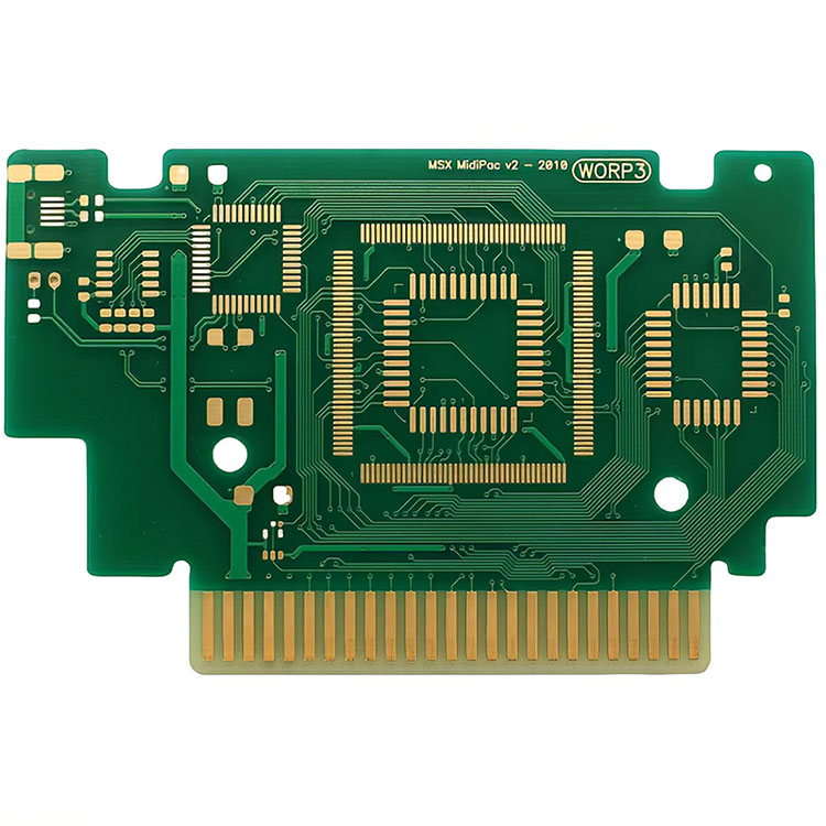
What is the process of multilayer PCB fabrication?
2024-06-14
Multilayer PCB (Printed Circuit Board) fabrication is a complex process involving several steps to ensure the creation of a functional and reliable PCB with multiple layers of conductive paths. Here’s a detailed breakdown of the multilayer PCB fabrication process:

1. Design and Preparation
- Schematic Design: Create a schematic diagram of the circuit using PCB design software.
- Layer Stack-up: Define the number of layers and the arrangement of signal, power, and ground layers.
- Design Rules: Establish design rules and constraints, such as trace width, spacing, and via sizes.
- Gerber Files: Generate Gerber files, which are the industry standard for PCB fabrication, including drill files and component placement files.
2. Material Selection
- Substrate Material: Choose the base material (typically FR4) and the copper foil thickness for the internal and external layers.
3. Inner Layer Preparation
- Imaging: Transfer the circuit pattern onto the inner copper layers using a photoresist and UV light. The photoresist hardens where the UV light hits, creating a protective layer over the copper.
- Etching: Remove the unprotected copper using a chemical etchant, leaving behind the desired copper pattern.
- Stripping: Remove the remaining photoresist to reveal the copper traces.
4. Layer Alignment and Lamination
- Alignment: Align the inner layers with each other and with the outer layers using optical equipment to ensure precision.
- Lamination: Stack the layers together with prepreg (a resin-impregnated fiberglass) between them. This stack is then placed in a laminating press, which applies heat and pressure to bond the layers into a single solid board.
5. Drilling
- Drill Holes: Drill holes through the stack for vias, pads, and mounting holes using computer-controlled drilling machines.
- Deburring: Remove any burrs or rough edges from the drilled holes.
6. Plating and Hole Preparation
- Electroless Copper Plating: Deposit a thin layer of copper on the walls of the drilled holes to ensure electrical connectivity between layers.
- Electroplating: Add additional copper to the holes and surface traces to build up the required thickness.
7. Outer Layer Imaging and Etching
- Imaging: Apply photoresist and use UV light to transfer the outer layer circuit pattern onto the copper foil.
- Etching: Remove the unprotected copper to create the final circuit pattern on the outer layers.
- Stripping: Remove the remaining photoresist to expose the copper traces.
8. Solder Mask Application
- Solder Mask Coating: Apply a layer of solder mask over the entire board to protect the copper traces and prevent solder bridges. The solder mask is usually a green epoxy, but other colors are available.
- UV Curing: Use UV light to harden the solder mask, exposing only the pads where components will be soldered.
9. Surface Finish
- Surface Finish Application: Apply a surface finish to the exposed pads to ensure good solderability. Common finishes include HASL (Hot Air Solder Leveling), ENIG (Electroless Nickel Immersion Gold), and OSP (Organic Solderability Preservative).
10. Silkscreen Printing
- Silkscreen Application: Print component designators, logos, and other information on the board using a silkscreen process.
11. Electrical Testing
- Automated Optical Inspection (AOI): Inspect the board for visual defects such as open circuits, short circuits, and misaligned traces.
- Electrical Testing: Perform electrical tests to ensure all connections are correct and there are no shorts or open circuits. This can be done using a flying probe tester or a bed-of-nails fixture.
12. Final Inspection and Quality Control
- Inspection: Conduct a final inspection to verify the PCB meets all design and quality specifications.
- Quality Control: Perform additional quality control tests as required by industry standards and customer specifications.
13. Cutting and Packaging
- Cutting: Separate the individual PCBs from the production panel using a router or a laser cutter.
- Cleaning: Clean the boards to remove any residual flux or contaminants.
- Packaging: Package the PCBs for shipment, ensuring they are protected from static discharge and physical damage.
The fabrication of multilayer PCBs is a meticulous process that requires precision and attention to detail at every step to ensure the final product functions correctly and reliably.


