

Top PCB Assembly Techniques for High-Quality Electronics Manufacturing
2026-06-09
In the fast-paced world of electronics manufacturing, the difference between a product that thrives and one that fails often lies in the precision of its PCB assembly. Whether you're developing a consumer device or a mission-critical system, mastering the right assembly techniques is non-negotiable. At TPS, we've seen firsthand how the right methods can elevate quality and reliability. This blog dives into the top techniques that redefine what's possible, sparking new ways to perfect your production—and leaving common pitfalls behind.
Mastering Precision Soldering for Flawless Joints
Achieving consistently perfect solder joints relies far more on finesse than brute force. Many newcomers assume cranking up the iron will speed things along, but that often backfires—excessive heat lifts pads, scorches flux, and stresses components. Instead, focus on dialing in a temperature that suits both your solder alloy and the board’s thermal mass. Let the tip linger just long enough to bring everything to a uniform working temperature, then watch how effortlessly the solder flows. That brief moment of controlled heat application separates a durable, shiny connection from a dull, unreliable one.
The choice of solder and flux plays an equally critical role. A quality 63/37 or lead-free alloy with a matching flux core simplifies wetting, but the wire gauge must align with the joint size—thin wire for delicate SMD work, thicker for through-hole. Don’t overlook the addition of external flux when reworking or tackling oxidized surfaces; it encourages that smooth, concave fillet that signals a solid metallurgical bond. Afterwards, inspect residues carefully. A quick wipe with isopropyl alcohol keeps ionics from plotting long-term corrosion under the prettiest joint.
Technique separates the artisan from the assembler. Keep the tip clean and generously tinned between joints to ensure rapid heat transfer. Touch the iron to both the pad and the lead simultaneously, count off a second or two, then feed solder from the opposite side—never from the tip itself. The resulting joint should glisten with a gently sloping meniscus, free of cracks, gaps, or witch’s hat points. A 10x loupe soon becomes your best ally, revealing details invisible to the naked eye and turning each connection into a minor testament of craftsmanship.
Optimizing Component Placement with Cutting-Edge Automation
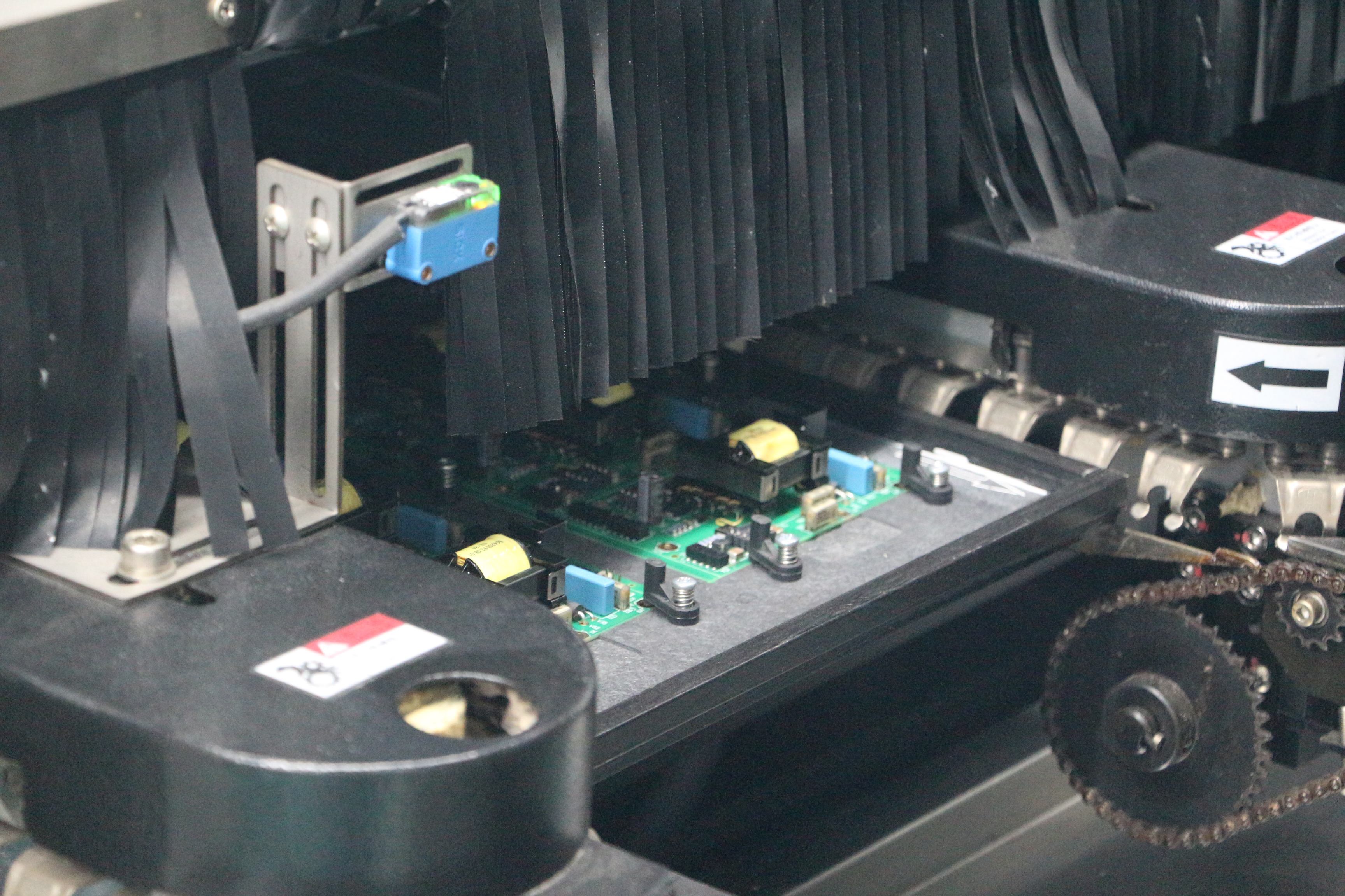
Modern electronics assembly lines are pushing the limits of speed and precision, and component placement is a prime target for innovation. Rather than relying on fixed programs that assume perfect conditions, advanced automation systems now interpret real-time sensor data to adjust on the fly. This shift means placement heads can correct for subtle board warpage or component drift without pausing the line, cutting down on the constant recalibrations that used to plague high-mix production.
What really sets newer systems apart is the fusion of high-speed imaging with tightly integrated feedback loops. Cameras snap sub-millisecond images mid-movement, while onboard processors compare each pickup and placement against live CAD data—not just a static library. This closes the gap between design intent and physical reality, catching orientation or offset errors that purely mechanical checks would miss. The result isn't just fewer defects; it's a dramatic reduction in the off-line rework that eats into yields and ties up skilled technicians.
Beyond the hardware, the software behind these machines has grown remarkably adaptable. Placement algorithms now factor in component scarcity and real-time supply-chain data to automatically resequence jobs or suggest alternative parts that fit within the same footprint. Over time, the system learns from cumulative misplacements, fine-tuning vacuum pressures, speeds, and approach angles for each package type without any manual intervention. This continual self-optimization turns a traditional bottleneck into a resilient, self-regulating process that keeps lines humming even as demands shift.
Ensuring Reliability Through Rigorous Inspection Protocols
Reliability isn't a feature you can simply add at the end of production—it's built into every stage of manufacturing through thorough inspection procedures. These protocols act as checkpoints, catching potential flaws early when they're easier and cheaper to fix. From the initial material checks to final assembly tests, each step is designed to verify that components meet strict specifications, reducing the chance of field failures.
Implementing rigorous inspection protocols means going beyond basic pass/fail tests. It involves detailed stress testing, environmental simulations, and real-world usage scenarios that push products to their limits. By replicating harsh conditions, we uncover latent weaknesses that standard quality checks might miss. This proactive approach helps refine designs and manufacturing processes continually, ensuring that every unit leaving the facility performs consistently over time.
Consistency is the cornerstone of trust. A well-documented inspection framework ensures that nothing slips through the cracks, regardless of who is on the line. Regular audits and calibration of inspection equipment maintain accuracy, while traceability records allow for rapid root-cause analysis if an issue does arise. Ultimately, these rigorous protocols are not just about catching defects—they're about building a culture of excellence where reliability is the natural outcome.
Implementing Effective Thermal Management Strategies
Effective thermal management is the unsung hero of modern electronics, often determining whether a device thrives or fails. As components pack more power into shrinking footprints, heat becomes a relentless adversary. Without careful planning, thermal runaway can degrade performance, shorten lifespans, or even cause catastrophic failures. The first step is always to map heat sources and thermal pathways within the system, treating airflows and conductive paths as critical design elements from day one.
The toolset for tackling heat stretches from simple passive sinks to pumped liquid loops, but the art lies in matching the method to the challenge. In tightly sealed enclosures, natural convection through finned heat sinks paired with strategic vent placement can work wonders. For high-density clusters, cold plates and coolant distribution units often prove indispensable. More recently, phase-change materials and vapor chambers have opened doors to compact, high-flux cooling that defies traditional limits, especially in mobile and edge computing.
Yet, the most forward-looking strategies weave thermal management directly into the product's DNA. Co-designing electrical and thermal systems, using simulation-driven layout optimization, and adopting materials with anisotropic thermal properties shift the focus from fighting heat to guiding it. The result isn't just a cooler device, but one that runs quieter, sips less energy, and withstands environmental extremes—hallmarks of truly refined engineering.
Enhancing Durability with Advanced Conformal Coating
Advanced conformal coatings do more than shield electronics from moisture and dust—they form a molecularly bonded interface that actively resists delamination under thermal cycling. Unlike standard acrylic or silicone layers, modern formulations incorporate nano-scale fillers and reactive groups that cross-link with substrate surfaces, creating a resilient barrier that maintains adhesion even when components flex or expand. This adhesion stability is critical for preventing micro-cracks that would otherwise allow corrosive agents to creep beneath the protective layer over time.
Durability gains are further amplified by coatings engineered to self-heal. Microcapsules or dynamic chemical bonds embedded within the polymer matrix can respond to minor scratches or abrasions, automatically resealing the protective envelope. This reduces the need for costly rework and extends the functional life of devices exposed to harsh environments, from automotive engine compartments to offshore wind turbines. The result is a shield that evolves with the stresses it faces, rather than simply wearing down.
Moreover, the application process itself has evolved to eliminate pinholes and uneven coverage, two common failure points in older spray or dip methods. Precision robotic dispensing and vapor-phase deposition ensure consistent thickness across complex geometries, even on sharp edges where stress often concentrates. By minimizing inherent weak spots during application, advanced coatings deliver uniform protection that directly translates to longer-lasting performance in the field.
Streamlining Rework to Maintain Product Integrity
Rework often feels like a step backward, but when it's unavoidable, the real challenge is keeping the product's original quality intact. Too many rushed fixes can introduce new flaws or weaken key components. Streamlining means building a smarter path from defect to correction—one that respects the product's design and materials at every stage.
A practical way to tighten this loop is by digging into the root causes without getting bogged down in paperwork. When teams have clear, uncluttered processes for logging issues and sharing feedback, they can spot recurring problems faster. This isn't just about speed; it's about creating a feedback culture where every rework moment becomes a lesson, not just a chore.
The real payoff comes when rework stops being a firefight and turns into a tuned part of the production rhythm. Products hold their intended strength and finish, customers notice the consistency, and the production floor wastes far less material and time. Over time, well-streamlined rework actually teaches you how to prevent it, lifting overall quality in ways that go beyond the immediate fix.
FAQ
Consistent quality in PCB assembly hinges on a combination of precise solder paste application, tightly controlled reflow profiling, and thorough inspection. For instance, using stencils with proper aperture design and thickness ensures consistent paste volume, preventing bridging or insufficient solder joints. Reflow ovens with multiple zones allow gradual thermal profiling tailored to specific board designs and component mixes, minimizing thermal shock. Automated optical inspection (AOI) catches defects like tombstoning or misalignment early, reducing rework. These techniques become even more crucial as component sizes shrink and board densities increase.
Mixed-technology boards introduce unique challenges because through-hole parts require different soldering processes than surface-mount components. Selective soldering has become the go-to solution here—it applies solder only to specific through-hole sites using a programmable nozzle, avoiding heat exposure for nearby SMT components. Alternatively, pin-in-paste (intrusive reflow) can be used: applying solder paste into through-holes and reflowing them together with SMT parts. Both methods demand careful process control to maintain joint integrity and avoid flux residues compromising long-term reliability.
Conformal coating acts as a protective barrier against moisture, dust, chemicals, and temperature extremes—common killers of electronics reliability. For assemblies deployed in automotive or industrial settings, a properly applied coating (e.g., acrylic, silicone, or urethane) prevents dendritic growth between conductors that leads to short circuits. Selective coating robots dispense the material with precision, avoiding connectors and areas that must stay uncoated. However, the real benefit shows under thermal cycling: coated boards withstand condensation and corrosive atmospheres much better than uncoated ones, extending service life significantly.
Heat dissipation directly impacts solder joint fatigue and component lifespan. Poor thermal management during assembly can cause warpage, delamination, or electromigration. Design choices like adding thermal vias under power components, using thick copper layers for current-paths, and specifying metal-core substrates for LED or high-power applications make a measurable difference. Additionally, the reflow process itself must consider the thermal mass of large components to avoid cold solder joints—sometimes requiring custom profiling with extended soak times. Ultimately, managing heat both during assembly and in operation prevents early field failures.
X-ray inspection is invaluable for examining solder joints that are optically hidden, such as those under ball grid arrays (BGAs), quad-flat no-leads (QFNs), or within press-fit connectors. Unlike AOI which only sees surface features, X-ray can detect voids, insufficient solder, bridging, and head-in-pillow defects. In high-reliability sectors like aerospace or medical devices, it’s often a mandatory step. The key is balancing resolution and throughput—3D X-ray systems (computed tomography) offer detailed slice images but are slower, while 2D systems provide faster inline checks for production monitoring.
DFM is not a one-time checklist but an ongoing collaboration between design and manufacturing teams. Early DFM analysis might flag acute trace angles that cause acid traps during etching, or component spacing that leads to shadowing during wave soldering. Modern DFM software runs rule checks on panelization, fiducial placement, and test point accessibility before prototype release. Sharing real-time data from the assembly line (e.g., pick-and-place machine errors, rework statistics) back to designers creates a feedback loop that eliminates recurring issues—like a specific package orientation that consistently causes tombstoning—cutting defect rates by double digits.
Conclusion
Achieving high-quality electronics manufacturing hinges on mastering a set of core PCB assembly techniques that blend precision, automation, and rigorous oversight. The foundation lies in flawless soldering—where controlled heat profiles and skilled technique eliminate cold joints and bridging, ensuring every connection remains robust under stress. This is complemented by cutting-edge automation for component placement, which leverages vision-guided systems to achieve micron-level accuracy even with miniaturized parts, drastically reducing human error. Together, these steps create a board that performs reliably from the first power-on, but they only represent the starting point for long-term durability.
True manufacturing excellence extends into comprehensive inspection protocols like automated optical and X-ray imaging, which catch latent defects before they escape the line. Thermal management then becomes critical: strategic use of thermal vias, copper pours, and heat sinks dissipates heat evenly, preventing hotspots from degrading sensitive components. To shield against environmental threats, advanced conformal coating is applied with selective precision, guarding against moisture, dust, and chemical exposure without adding bulk. When issues do arise, a streamlined rework process—using focused hot-air stations and controlled desoldering—allows corrections that maintain the product’s original integrity rather than compromising it. These interconnected practices elevate PCB assembly from routine production to a disciplined craft that meets the demands of modern electronics.
Contact Us
Contact Person: Lily
Email: [email protected]
Tel/WhatsApp: +49 (0) 2161 49526-0
Website: https://tps-elektronik.com/en/