

China Semiconductor Equipment Connector Demand Drives New Precision Manufacturing Standards
2026-11-17
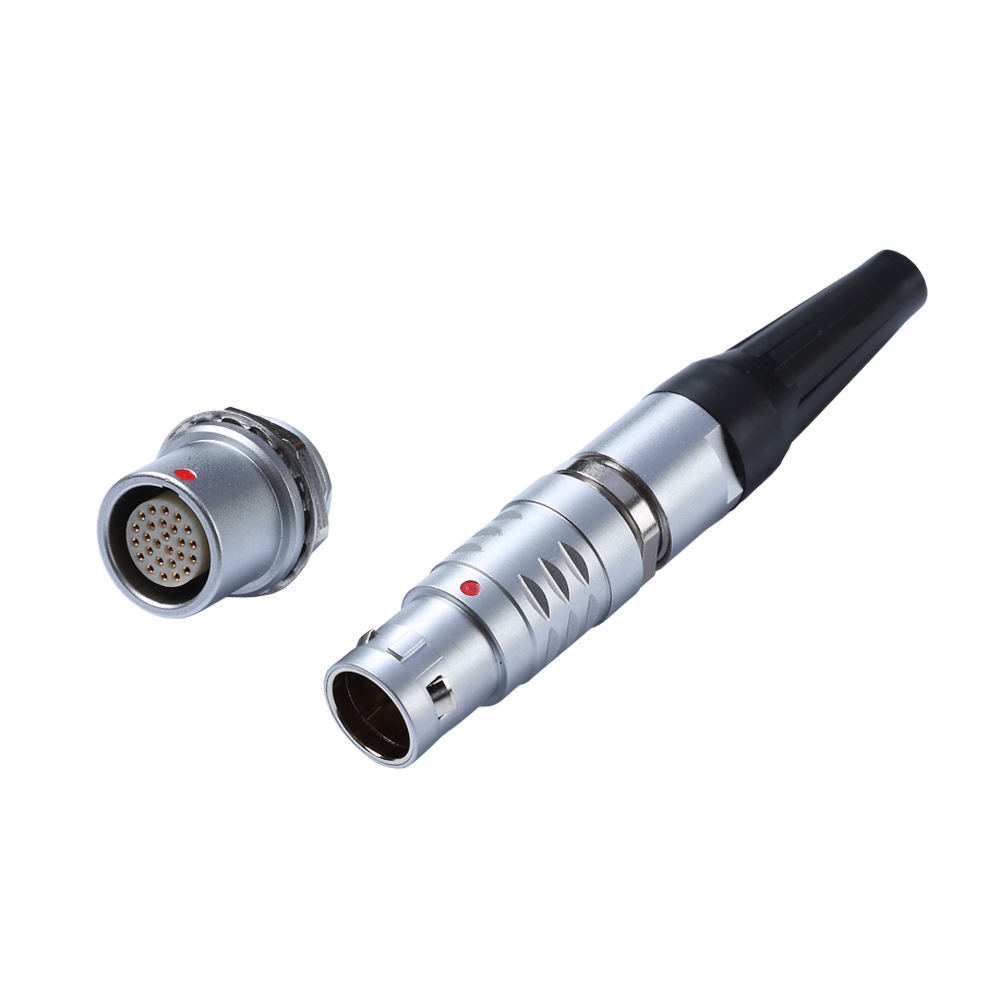
Demand for semiconductor equipment connectors in China is beginning to set the pace for precision manufacturing, not just follow it. That inversion is forcing equipment makers to replace long-held assumptions about tolerances, plating consistency, and cleanroom handling with measurable, repeatable standards. The reason is straightforward: a connector that drifts in the field can idle a tool costing far more than the part itself. At REUNION, this shift shows up in tighter incoming inspection data and more demanding customer specifications. What follows explains why connectors have become an unlikely leverage point for China's semiconductor equipment supply chain.
Surface Finish Specs Now Show Up in Yield Models
For a long time, yield predictions leaned on electrical test data, critical dimensions, and defect density while surface finish sat in a separate quality bucket. That split often meant a part could pass its roughness or flatness checks yet still contribute to downstream failures that the model never saw coming. Now those surface finish parameters are being pulled directly into yield models, giving process teams a clearer line of sight from wafer topography to final device performance.
The shift is more than a data merge. Roughness, waviness, and localized flatness readings are being treated as continuous variables rather than pass/fail flags, so the model can weigh how a slight change in Ra or a subtle edge rolloff affects the probability of good die. Engineers can finally see which surface characteristics actually move the needle instead of guessing whether a polish step or a film deposition tweak is worth the cost.
In practice, this means fewer late-stage surprises. When a lot drifts toward the edge of the finish spec, the yield model flags the risk before the material moves further down the line. Teams can adjust tooling, slurry conditions, or cleaning steps while there is still time, reducing scrap and making design rules around surface finish less of a paper exercise and more of a live production lever.
Chinese Fabs Want Cleanliness Data, Not Just Compliance Paper
Chinese semiconductor fabs are shifting away from a paper-driven compliance mindset. For years, cleanroom certifications and particle count reports existed mainly to satisfy audit checklists. Now, process engineers and facility managers want live telemetry from particle counters, humidity sensors, and chemical monitors that feeds directly into their yield analysis tools. A signed certificate that says the cleanroom was within spec last month is no longer enough when a single micro-contamination event can scrap a wafer lot worth hundreds of thousands of dollars.
This demand for real cleanliness data is changing how vendors and fab owners evaluate monitoring systems. Instead of asking whether a system meets ISO 14644-1 at commissioning, teams now ask how often data is sampled, whether it can be correlated with specific process steps, and how easily it can be exported to statistical process control dashboards. The goal is not to prove cleanliness on paper, but to catch drift, filter saturation, or unexpected particle bursts before they impact production. In many advanced fabs, the cleanroom monitoring network is now treated as a production tool rather than a compliance overhead.
Equipment suppliers are responding by integrating edge computing and time-stamped data logging into their sensors. Rather than offering monthly or quarterly certification reports, they provide continuous particle concentration trends, temperature and humidity overlays, and alarm histories tied to specific tools or operators. Fab engineers increasingly expect the same level of data granularity they get from lithography or etch equipment. In this environment, a cleanroom that only produces a compliance paper is seen as a black box, while one that streams actionable cleanliness data becomes part of the yield improvement loop.
Tighter Mating Tolerances Push Machining Past Legacy Limits
As mating part tolerances collapse below what legacy machines were rated to hold, shops discover that thermal growth in a spindle or a few millionths of tool deflection can consume the entire tolerance band. The old habit of running a warm-up cycle and trusting a post-process inspection no longer works. Instead, machinists are mapping error sources across the day, adjusting offsets from in-machine probing data, and re-qualifying setups after short idle periods.
This shift changes how workholding and tooling are specified. Hydraulic vises, shrink-fit holders, and balanced boring heads once considered overkill now show up on ordinary production lines because they remove small variables that legacy clamping methods leave behind. Shops also lean on controlled shop air, spindle chillers, and slower finish passes not to chase surface finish, but to keep part dimensions stable long enough for measurement to reflect true geometry.
The practical result is less about buying a single high-end machine and more about rebuilding the process around the tolerance. Older equipment can often hold tighter mating fits if the operator shortens measurement loops, compensates for drift before it becomes a reject, and treats every setup as a source of variation rather than a fixed reference.
Submicron Metrology Becomes Standard Incoming Inspection
For years, receiving inspection stopped at gross dimensional checks—calipers, go/no-go gauges, maybe a height stand. But when features drop below a micron, that approach falls apart quietly. Submicron metrology has moved out of the lab and into the dock because vendors can no longer assume a part is good just because it fits a fixture. Optical profilers, white-light interferometers, and high-resolution CMMs now sit next to the receiving bench, checking form, roughness, and coating thickness before inventory is accepted.
The shift is less about owning fancier instruments and more about making them routine. Current systems handle vibration, temperature drift, and focus routines well enough that an incoming inspector without a metrology background can load a tray, call up a part number, and get pass/fail data in minutes. That removes the bottleneck where parts waited days for lab time, and it catches surface defects or edge rounding that traditional contact gauges simply miss.
A practical result is that the boundary between supplier and buyer has become tighter. Data from incoming measurements is shared back to machining or coating teams, so tolerance drift is corrected before it becomes a formal rejection. In many plants, submicron inspection is now written into the purchase order as standard practice, not as a special request—making it a normal gate rather than an occasional audit.
Thermal Drift Tests Are Moving to Tool-Level Conditions
Thermal drift characterization used to live mostly in the reliability lab, where small samples were soaked in ovens or placed on thermal chucks and measured over long intervals. The data was useful for understanding material behavior, but it often missed what happens when a device sits in an actual production test socket with forced air moving across the load board. As a result, drift numbers that looked acceptable on a bench setup occasionally turned into test yield shifts or guardband failures on the floor.
Moving these tests to tool-level conditions means the device is no longer treated as an isolated specimen. The socket body, handler thermal head, pogo pin resistance, and even the PCB trace heating all become part of the measurement loop. Engineers now look for small parameter movement during continuous cycling, insertion repeats, or soak periods inside the handler, rather than relying on a single stabilized junction temperature. This catches contact-related drift and local thermal gradients that a uniform oven simply cannot reproduce.
The shift also changes what gets recorded. Instead of one drift value per temperature step, teams track drift against thermal settling time, across multiple insertions, and under production airflow. That data feeds directly into guardband decisions and helps separate true device behavior from tool-induced noise. It is a noisier measurement and it takes longer to set up, but it reflects the environment where the part actually has to pass.
High-Vacuum Connector Materials Get Scrutinized Earlier
Material decisions for high-vacuum connectors rarely wait for the vacuum test bay anymore. Teams now pull candidate insulators, shells, and seal compounds into a short screening loop long before the first prototype bake-out. The focus lands on outgassing rates, trapped volatile content, and thermal cycling behavior, because a connector that looks clean on a bench can dominate residual gas once it reaches 10^-6 mbar.
Suppliers have adjusted to requests for batch-level data rather than generic compatibility claims. A polyimide or PEEK insulator may pass a datasheet review but still carry moisture from machining or cleaning. Early scrutiny includes residual gas analysis on small assemblies, with attention to plasticizers, cutting fluids, and o-ring lubricants that do not show up in dimensional inspection.
This earlier review changes the conversation from pass/fail compatibility to outgassing budget. Design teams compare materials under the same pressure and temperature window, then run thermal soaks on short connector stubs before committing to a full harness. The result is fewer late-stage material swaps and less rework when the chamber finally reaches its base pressure.
FAQ
The move toward finer interconnect pitches and higher pin counts means a few microns of deviation can now create signal integrity problems or misalignment during wafer handling. Equipment builders are asking suppliers to hold positional tolerances that were considered optional just a few years ago.
Beyond tighter dimensional control, the new expectations cover burr-free contact edges, cleaner plating thickness distribution, and more consistent spring force across high-mating-cycle connectors. Manufacturers are also being required to document process capability instead of relying on final inspection alone.
Many are investing in Swiss-style turning, laser welding, and automated optical inspection to reduce batch variation. Some have started co-developing connector layouts with equipment teams earlier in the design cycle, which shortens qualification time but puts more pressure on engineering resources.
Vacuum environments in deposition and etch tools are especially unforgiving. Connectors there must avoid outgassing, hold up under thermal cycling, and maintain low contact resistance without traditional lubricants, which pushes suppliers toward specialized platings and cleaner assembly methods.
Both. Beryllium copper remains common for spring contacts, but suppliers are testing alternative alloys and higher-purity copper to balance conductivity with fatigue life. Insulator materials are also being reviewed for lower moisture absorption and better dimensional stability after baking.
They are qualifying second sources more aggressively and asking local suppliers to match foreign datasheets rather than offering relaxed copies. That creates a faster feedback loop between connector failures in the field and design revisions, but it also raises the cost of wrong assumptions early in a program.
Likely yes, because global equipment makers often share qualification requirements across regions. Once a Chinese fab or tool supplier proves a tighter standard is achievable, it can become a reference point for other markets, especially where advanced packaging and high-density interconnect are growing.
Conclusion
Connector suppliers serving China’s semiconductor equipment market are being pulled into yield and process-control conversations far earlier than in the past. Surface finish specifications, once treated as routine drawing notes, now appear directly in yield models because micro-roughness, plating voids, and edge burrs can shift particle counts and contact resistance in etch, deposition, and metrology tools. Chinese fabs increasingly ask for raw cleanliness data such as particle counts, outgassing readings, and ionic contamination levels instead of accepting a certificate of compliance at face value. That demand is forcing connector makers to apply cleaner machining and packaging workflows and to maintain lot-level traceability through cleaning and drying steps. At the same time, tighter mating tolerances are pushing precision machining past legacy limits. Standard Swiss turning and conventional grinding often cannot hold the required geometrical control, so suppliers are investing in temperature-stabilized cells, custom fixtures, and in-process measurement to keep pin position and contact alignment repeatable.
Incoming inspection at advanced fabs has shifted toward submicron metrology as the default gate. Profilometry, interferometry, and automated optical inspection are now used to verify pin geometry, surface texture, and contact area before connectors reach the production floor. Thermal drift testing is also moving from simple oven soak tests to tool-level conditions that replicate chamber cycling, RF heating, and vacuum bake-out. A connector that looks stable on a bench can still shift enough inside a process module to affect alignment or contact force. High-vacuum connector materials receive earlier scrutiny as well, with design reviews now examining hydrogen outgassing, plating adhesion, and particle shedding under thermal stress before prototypes are approved. The practical result is that connector makers are no longer selling dimensional compliance alone. They are expected to supply metrology data, process-control evidence, and lifecycle behavior that directly supports fab yield and tool uptime, and that expectation is reshaping how precision machining suppliers qualify materials, run production batches, and document their work.
Contact Us
Contact Person: Hayley Liang
Email: [email protected]
Tel/WhatsApp: +86 13480625451
Website: https://www.reunion-china.com/